Software
IBM Achieves 0.7nm Chip Breakthrough with NanoStack Architecture
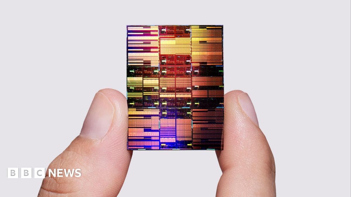
IBM Achieves Historic 0.7nm Chip Breakthrough
IBM has unveiled a revolutionary chip design that could fundamentally reshape the semiconductor industry. The company's new NanoStack architecture reportedly achieves the equivalent of 0.7 nanometres — making it the industry's first known chip technology below the critical 1nm threshold.
The Challenge: Horizontal Scaling Hits a Wall
For decades, Moore's Law has driven the semiconductor industry forward by cramming more transistors onto silicon. The current industry standard sits around 2nm (nanometres, billionths of a metre). But physical limits are approaching fast.
Instead of continuing to shrink transistors horizontally, IBM's approach is radically different: build upward.
The NanoStack Solution: A Skyscraper Approach
Rather than placing transistors side-by-side, IBM's NanoStack architecture layers them vertically, creating what computer scientist Professor Alan Woodward at Surrey University aptly describes as "a 100-storey skyscraper" of circuitry.
"IBM's NanoStack is like proposing a 100-storey building, while Samsung and Intel are closer to 30-50 storey buildings with their own 3D chip work," Woodward explained.
Performance Gains
In testing, IBM's prototype demonstrated:
- 50% better performance than its own 2nm chip
- 70% improved energy efficiency
- Potential to cram 100 billion transistors on a fingernail-sized chip
The Engineering Challenge
Vertical stacking isn't straightforward. Heat dissipation becomes critical — transistors generate warmth as they operate, and heat rises. Thinner layers between stacked transistors can also cause unwanted leakage, preventing circuits from switching off properly.
Jay Gambetta, director of IBM Research, called it a "landmark moment" for chip design: "We're not just making smaller transistors, we're reinventing how chips are built."
Timeline: Years Away from Production
While impressive, IBM acknowledges the technology won't reach commercial production for several years. The prototype proves the concept, but scaling to mass manufacturing requires solving thermal management, reliability, and yield challenges.
Still, it's a significant milestone in the race to extend Moore's Law and maintain exponential performance gains in computing.
Source: BBC News
Comments
Loading comments...